Perovskite solar cells
Metal halide perovskites attract considerable attention for application in photovoltaic cells. These materials have an ABX3 crystal structure where A is a monovalent cation, B is metal dication, and X a halide anion. The first perovskites used for solar cells consisted of methylammonium, lead, and iodide (CH3NH3PbI3) but in the meantime many more complex metal halide perovskites have been developed in which other organic or inorganic cations, different metals, and multiple halides are used. These perovskites can be processed from solution into thin films in one- or two-step procedures and afford very efficient solar cells. The highest reported efficiencies already exceed 26%. However, the materials pose several scientific and technological questions, regarding their operational mechanism, stability, and opportunities to further increase the efficiency.
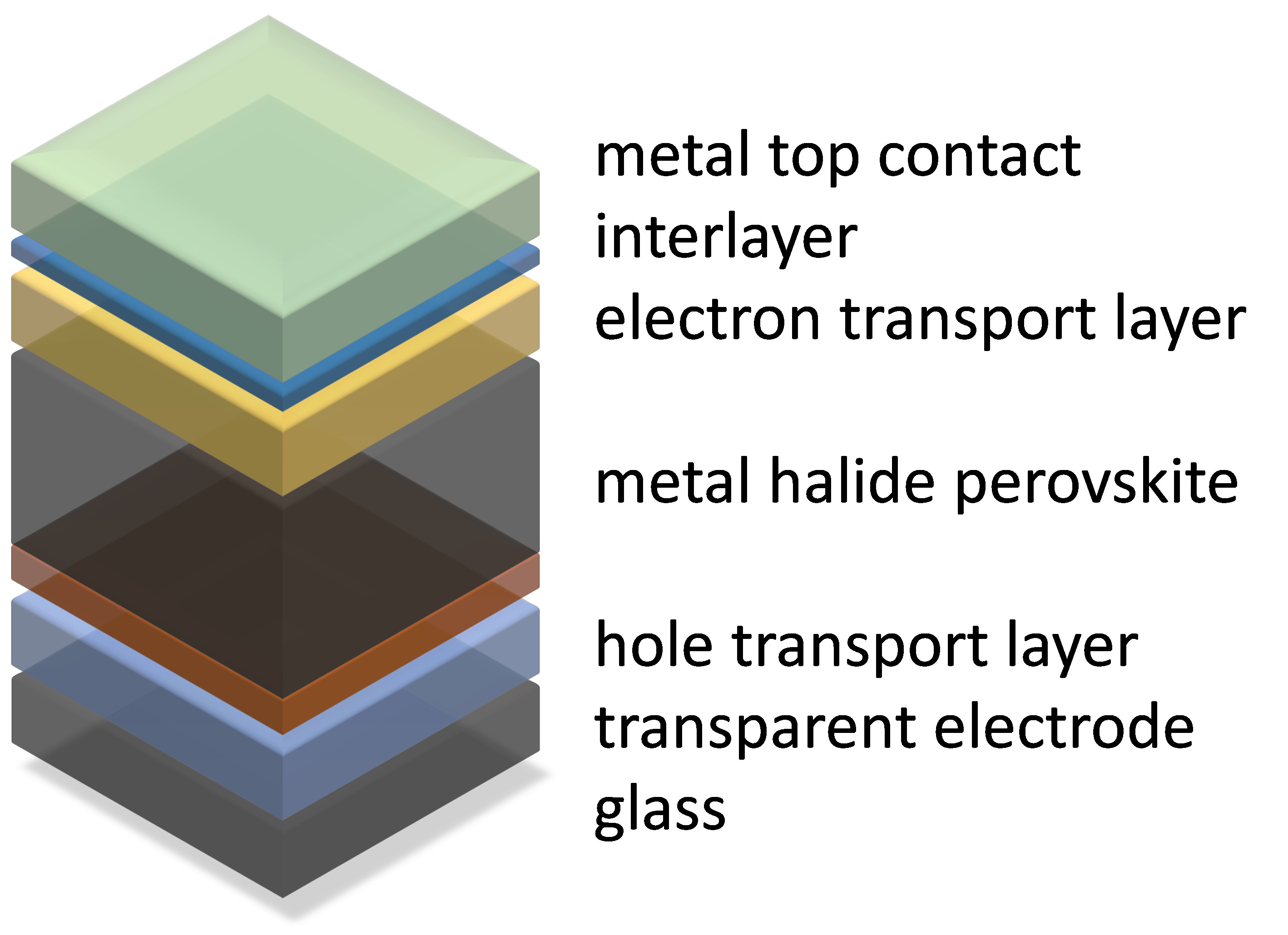 Layout of a thin film metal halide perovskite solar cell
With the M2N group we investigate perovskite solar cells from different perspectives:
Band gap tuning
The CH3NH3PbI3 perovskite has a band gap of about 1.55 eV. Tuning of the band gap can be accomplished in several ways and can be very beneficiary. For example for the development of tandem solar cells two different band gap materials are needed and this can be accomplished by tuning the perovskite structure. Also indoor photovoltaic applications will require tailored absorber layers. By partially replacing lead by tin one can achieve band gaps as low as 1.21 eV, while by replacing iodide by bromide, the band gap can be increased to 2.32 eV. Another way of tuning the perovskite is by changing the dimensionality of the crystal. These are known as 2D Ruddlesden-Popper perovskites in which one or more perovskites layers are isolated from each other by the large spacer cations. Each new perovskite poses new challenges with respect to processing into thin and smooth layers, stability, and charge transport layers that allow extraction of electrons and holes without energy loses.
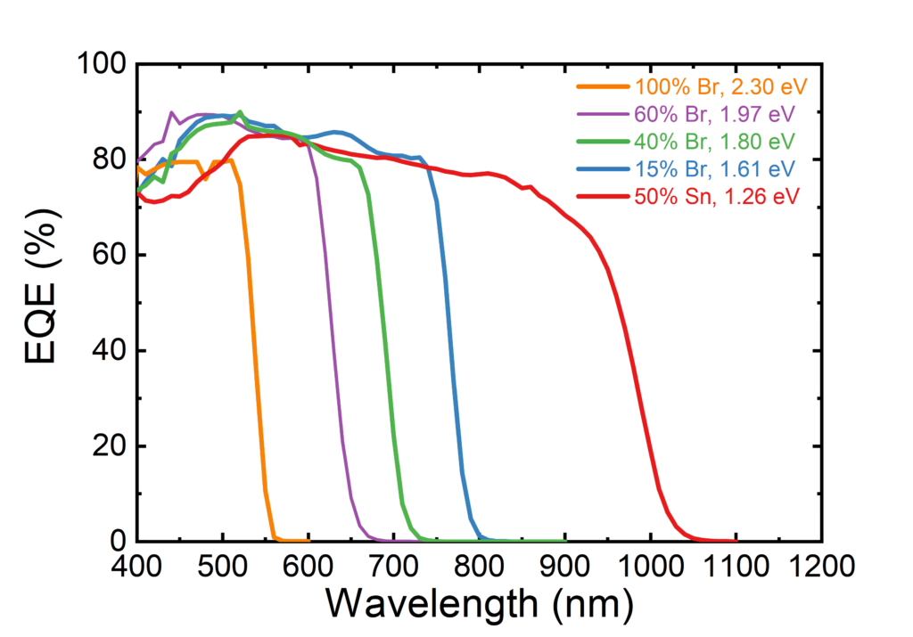 External quantum efficiency of metal halide perovskite solar cells with different band gaps
We develop new perovskite semiconductors, investigate these with a range of techniques such as X-ray diffraction, scanning electron microscopy, photoelectron spectroscopy, and fabricate and characterize solar cells based on these materials.
Multi-junction solar cells
To eventually surpass the 33.7% Shockley-Queisser limit for single solar cells junctions a well-knows strategy is to stack multiple cells with different band gaps. Obviously this requires absorber layers with different band gaps. We investigate both perovskite-perovskite, perovskite-silicon, and perovskite-CIGS tandem cells in two-terminal or four-terminal device configurations. To maximize light absorption and power conversion efficiency, we perform optical simulations on to design stack in order to reduce parasitic absorption and reflection losses. Especially for a two-terminal configuration a challenge is achieve current matching but also to fabricate the cells. Sometimes ten or even more layers must be stacked on top of each other. In case of solution processing this requires careful optimization and design of materials a processing steps.
Among the first groups in te world we have been able to report efficient triple-junction perovskite solar cells (Nat. Commun. 2020) and together with TNO we have set a new world record for four-terminal perovskite – crystalline silicon (c-Si) tandem solar cells with an efficiency of 30.1%. In monolithic tandems cells we have made 23.1% all-perovskite tandems (Adv. Mater. 2022) and 25.1% perovskite/c-Si tandem cells together with TU Delft.
Detection of defect states
Next to enhancing performance by improving materials and designing new device architectures, we study fundamental properties of these materials. Perovskites are known to have defects that may come as interstitials, vacancies, impurity atoms, lattice defects, phase separation, grain boundaries and others. On top of this, these defects are known to be dynamic: they can be mobile or change with time or operating conditions. One of the failure mechanisms is related to light-induced halide segregation in mixed halide perovskites which is studied both experimentally and theoretically (Nat. Commun. 2021). Some defects are important to the operation of the solar cells because they cause non-radiative recombination of electrons and holes that were generated by light. This non-radiative recombination causes a loss in the open-circuit voltage and to mitigate these effects it is necessary to understand in detail their nature. For this we employ different techniques such as electroluminescence, impedance spectroscopy, and photothermal deflection spectroscopy. We further developed an ultra-sensitive photocurrent spectrometer that is used in combination with optical modelling to unravel the location and nature of defects (Nat. Commun., 2022). We have also implemented home-built set ups to study quasi-Fermi level splitting optically. With these techniques we can unravel the factors that currently limit performance.
Contact
René Janssen
Martijn Wienk
Polaritons in organic semiconductors
Molecular semiconducting materials that strongly absorb visible and near infrared light are used in organic solar cells. For wavelengths near an allowed optical transition, crystals of dye molecules usually show high reflectance. This seems at first sight to preclude efficient absorption of light by the crystals. However upon closer inspection, the reflection band of these crystals near the allowed transition shows a minimum in reflectance in the middle of the band. This minimum can be assigned to polaritons. The polaritons arise from the strong coupling between electromagnetic waves with electronic polarization and excitation waves of the molecules. The polaritons allow for efficient in-coupling of light into organic crystals.
Within M2N we study fundamental properties of polaritons in organic crystals:
Upon illumination of the crystal at a wavelength corresponding to the excitation of polaritons at the minimum in the middle of the reflection band, light should be able to enter the crystal efficiently. Transport of the energy by the polariton to the interface with a second crystal can in charge carrier generation. The generation of carriers in turn should result in a photovoltage and/or a photocurrent. The external quantum efficiency spectrum of this photovoltaic action is to show a maximum at the wavelength associated with the minimal in reflection, providing direct evidence for the involvement of polaritons in the photovoltaic response.
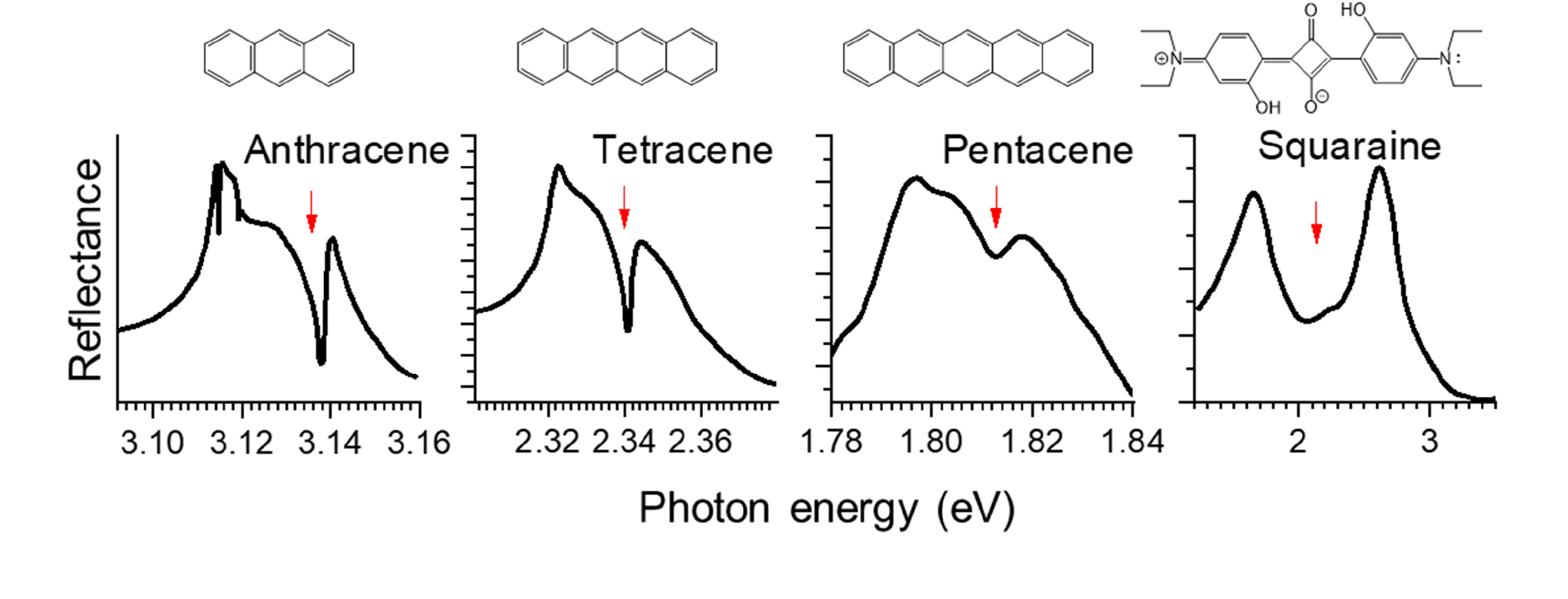 Reflection spectra for some crystals of organic dye molecules. The red arrow indicates the local minimum in the middle of the reflection band associated with the excitation of polaritons
Contact
Stefan Meskers
 Tandem-like photodiode that can measure a heartrate from a finger at a distance from the reflected near infrared light (Photo: Bart van Overbeeke)
 Tandem-like photodiode (Photo: Bart van Overbeeke)